News & Blog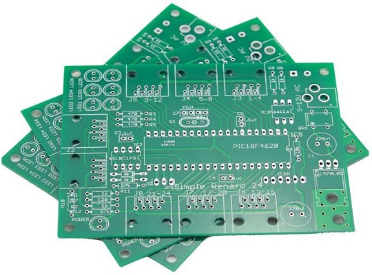
Comparison of several PCB surface finish typesMonday,Aug 13,2018
Comparison of several PCB surface finish typesAs for the essential proceed in PCB production, the basic purpose of surface treatment is to ensure good solderability or electrical properties. Since copper in nature tends to exist in the form of oxides in the air, it is unlikely to re... 
Via-in-Pad PCBTuesday,Jul 10,2018
PCB Via-in-PadWhen it comes to Vias, it’s known to us all that Vias can be divided into Through-hole Vias, Blind Vias and Buried Vias. They have different functions.With the development of the electronic products, Vias play a vital role in the interconnection between layers in a... 
Guideline for wire bondingTuesday,Jun 12,2018
There are two wire bonding processes that are used,Thermosonic (T S)Gold Ball Wire BondingandUltrasonic (U S)Aluminum Wedge Wire Bonding Approximately 90% of all IC Assembly in Semiconductor Packages is manufactured using Gold Ball Bonding process, while Aluminum Wedge Bonding is used to 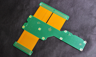
What is the Advantages of Rigid-Flex PCB?Tuesday,May 22,2018
WHAT IS RIGID-FLEX PCB?Rigid-flex PCB is a printed circuit consisting of both flexible circuit and rigid circuit This combination is ideal for exploiting the benefits of both flexible and rigid circuits - the rigid circuits can carry all or the bulk of the components, with the flexi 
BGA Advantages and DisadvantagesTuesday,Apr 10,2018
Ball Grid Array orBGAis asurface-mount package(with no leads) utilizing an array of metal spheres (solder balls) for electrical interconnection BGAsolder balls are attached to a laminated substrate at the bottom of the package The die of theBGAis connected to the substrate by wire bondi 
How to improve EMC performance on 8 layer PCB design?Tuesday,Mar 13,2018
8 Layer PCB Stack-up GuidelinesHow to improve EMC performance on 8 layer PCB design?The following text is reproduced, with permission, from Part 4 of a 6-Part article on PCB Stackup by Henry W Ott The original article is available athttp: www hottconsultants com tips htmlAn eight-layer 
High Frequency PCB Design TechniquesTuesday,Jan 16,2018
Author: David JonesHigh frequency design is where you really need to consider the effects of parasiticinductance, capacitance and impedanceof your PCB layout If your signal is too fast, and your track is too long, then the track can take on the properties of a transmission line If 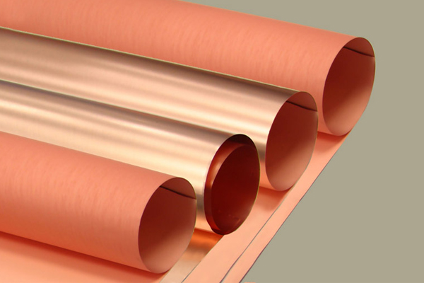
PCB prices may rise on copper foil shortage in 2018Friday,Dec 08,2017
With several governments desiring a shift towards cleaner new-energy vehicles, and an all-electric automotive indust... 
Plated-through slotsTuesday,Nov 14,2017
Plated-through slots1. The definition of plated slot For a board, it may contain plated slot or unplated slot. Plated slot means this slot is plated with copper which can be used for electrical connection.2. Pictures to show3. Size of plated slotThe min side of plated slot is 0.5mm... 
Which PCB testing method is better for you?Wednesday,Oct 04,2017
Very often, customers ask details about what kind of testing do we use? How do we charge it? Do I have to pay every time or only for the first time? Isthis testing safer and better than other one? etcIn this blog, let& 39;s discuss the various kind of testing and their advantage |


